Hi.
So you’re now taking the Digital Logic class1.
If you’re less familiar with computer science and engineering, you might think to yourself,
“great, I’ll be doing some beep boop bop 🤖 binary things this term”.
You’d be right.
In class, you’ll learn boolean logic theory.
In labs, you’ll see how that theory can be used to make something more concrete with VHDL.
This primer assumes you’re familiar with boolean algebra using basic AND, OR, and NOT gates.
What is VHDL?
VHDL is a programming language to describe circuits. It literally stands for: VHSIC (yes another acronym–don’t sweat it) Hardware Description Language. VHDL targets digital circuits in contrast to analog circuits. Digital circuits consider discrete logical properties like 1’s and 0’s, Yes’s and No’s. Analog circuits consider continuous electrical properties like voltage, impedance, capacitance, et al. This is a generalization but will hold true as far as an introductory course is concerned.
Here’s a taste of VHDL:
ENTITY inverter IS
    PORT ( in1 : IN BIT; out1 : OUT BIT );
END inverter;

ARCHITECTURE df OF inverter IS
BEGIN
    out1 <= NOT in1;
END df;
<= is an assignment operator in VHDL. It is not less than or equal to like in some other languages.
Although the syntax is a bit clunky, you can see how we’re just defining an inverter; a NOT gate.
First, we declare the inputs and outputs of our circuit block.
Then, we describe how the input is transformed into the output.
We’re describing the following equation:
Amaaahzing right? Later on we’ll go into more details on the syntax.
Why is VHDL?
Why would we want to model digital circuits? It’s easier to understand, modify, simulate, and test our designs by modeling our circuits in VHDL. VHDL (or any HDL) provides a common language that can be used at each of these stages, leading up to the final logic synthesis and layout steps, required to continue towards physical manufacture the design. During the digital logic design phase, VHDL allows us to treat circuit components as black boxes so we can build up more complex and powerful circuit designs.
How is VHDL?
Many of you will have been exposed to a programming language at this point. VHDL and other HDLs can be thought of as a programming language for digital circuits:
| HDLs | Traditional Programming Languages |
|---|---|
| VHDL, Verilog, SystemC, Bluespec | Python, Matlab, C, Javascript, R, Racket |
| Describes computation as a combination of digital circuits | Describes computation a set of steps for the computer to execute (imperative programming) |
| Building blocks from boolean algebra | Building blocks from arithmetic |
Ordering in VHDL
Before we move on, let’s distinguish one more difference between VHDL and the imperative programming languages you’ve probably seen in the past. Imperative programming languages are based on the idea of sequential statements. In other words, steps are executed one after the other in the order they appear. For example, we can assign a value in one step and read it back in consecutive steps.
# pseudo-code
a = 5
b = a + 1
b  # b == 6
In VHDL, we model circuits, so data just propagates through signals (usually we can think of them as just wires).
ENTITY pass_through IS
    PORT ( a    : IN BIT;
           b, c : OUT BIT);
END pass_through;

ARCHITECTURE df OF pass_through IS
    SIGNAL between : BIT;
BEGIN
    -- b and between are set
    -- at the same time!
    b <= between;
    between <= a;
    c <= between;
END df;
If we read the above example like a sequential program,
it looks like between is being assigned to b before between has any value!
We don’t set between until the next line.
However, when we go to run the circuit, we’ll see b and c will have the same value at the same time.
This is because we’re just connecting signals together, and the value of a is just passing through
our circuit to the other signals.
In digital logic terms, this is called a fan-out.
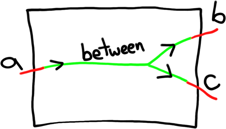
When we simulate this circuit all of our 1’s and 0’s flow through the circuit in a real-time(ish) way.
We’ll explain how to use VHDL with a short example.
Designing a Thing
Step 1. Understand the Problem
We’ll make a basic selector circuit that selects between one of two signals. You may have learned about this circuit already, called a (2x1) mux.
When the selector is off, the zeroth signal is selected.
When the selector is on, the first signal is selected.
Easy-peasy.
Step 2. Generate an Equation
Above, we’ve declaratively described a simple mux with text. It will be easier to implement the mux in VHDL from a formal equation, so that we can map the operations in the equation (AND, OR, NOT, et al) to basic gates in VHDL.
Eventually, you’ll be able to generate the equation directly from intuition. For now, let’s go through the process of making a truth table for all possible input combinations:
| (zeroth signal) |
(first signal) |
||
|---|---|---|---|
| 0 | 0 | 0 | 0 |
| 0 | 0 | 1 | 0 |
| 0 | 1 | 0 | 1 |
| 0 | 1 | 1 | 1 |
| 1 | 0 | 0 | 0 |
| 1 | 0 | 1 | 1 |
| 1 | 1 | 0 | 0 |
| 1 | 1 | 1 | 1 |
We’ll be verbose while simplifying our equation, for demonstrative purposes. If you’re able to jump right to the final equation, that’s great!
If we analyze the textual description, we can see how we’d intuitively generate our equation. When is 0 (off), our will be 0 if is 0, and 1 if is 1. The same can be said for when is 1 (on). If it’s not clear how that leads to equation \eqref{mux:final}, don’t sweat it.
In either case, make sure to check the actual indices (such as 0 or 1) and use common sense when implementing a circuit.
Step 3. Sketch out a Schematic
Sketching a schematic of our equation will help when translating our equation (read: circuit) into VHDL. It helps us identify all the pieces we’ll need to use in our VHDL code, e.g. inputs, outputs, intermediate signals, boolean gates, et al. A drawn schematic is not always required, but can help when we’re feeling lost and need to organize the problem.
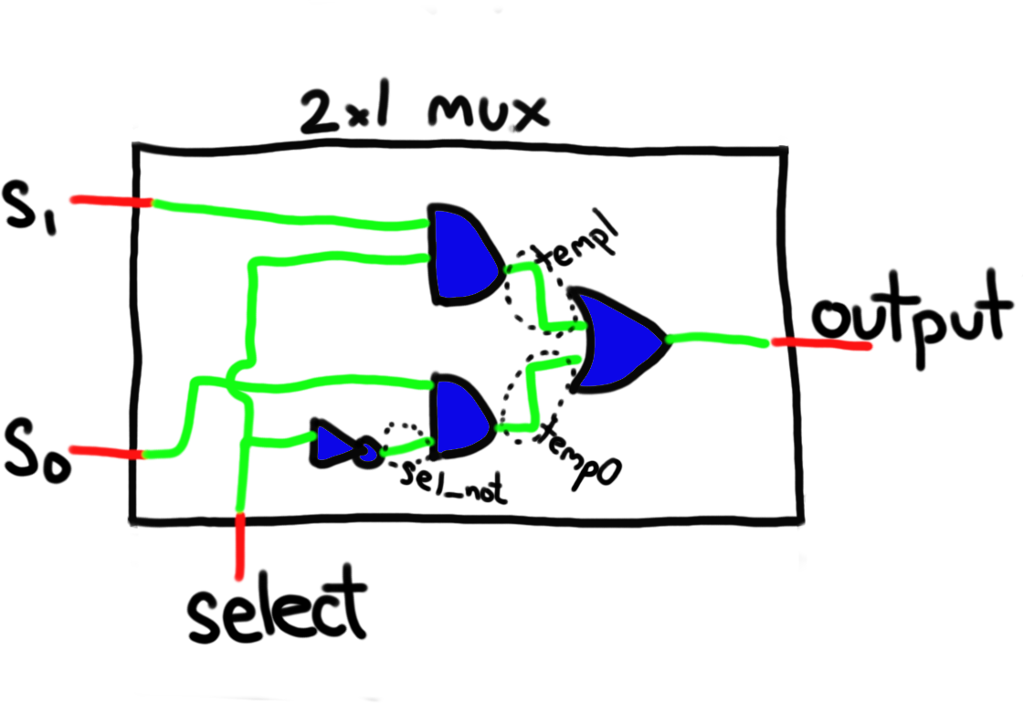
We’ve made a…box (helpfully color coded)!
- First, we labeled all our inputs and outputs. That might seem obvious, but it’s important to establish the interface to our box.
- Second, we filled in our other components. Sometimes our components will be other complex circuits that have inputs and outputs. In this circuit, our components are basic gates–AND, OR, and NOT.
- Last, we made sure everything had a name. That includes all the “wires”, or signals, in our design. If we had more complex components other than AND, OR, and NOT, then we would make sure that those were named, too. (We’ll see an example of that later on.) If a signal is directly connected to an input or output we can just use the name of that input or output. Some of our signals just exist between our gates, so we give those names (sel_not, temp0, temp1).
Great! Now we can code up our circuit!
Step 4. Implement it in VHDL
We just have to map our schematic to our code:
1
2
3
4
5
6
7
8
9
10
11
12
13
14
15
16
17
18
-- Comments start with '--'
-- Inputs and Outputs
ENTITY mux_2x1 IS
    PORT ( sel : IN BIT;
           s0  : IN BIT;
           s1  : IN BIT;
           output : OUT BIT
         );
END mux_2x1;

ARCHITECTURE df OF mux_2x1 IS
    SIGNAL sel_not, temp0, temp1 : BIT;
BEGIN
    sel_not <= NOT sel;
    temp0 <= sel_not AND s0;
    temp1 <= sel AND s1;
    output <= temp0 OR temp1;
END df;
Let’s unpack this one piece at a time.
In the above example, the highlighted code differentiates between:
- keywords like
ENTITY,ARCHITECTURE, andBEGINwhich denote the structure of our code. - identifiers like
s1,a,mux_2x1, anddf, which are just names we’ve chosen for different parts of our design. - operators like
<=,AND, et al, which can create and set values referenced by identifiers.
mux_2x1, MUX_2X1, mUX_2x1, etc all refer to the same identifier.
In the examples shown, I made keywords ALL-CAPS and identifiers lower-case, to differentiate them.
In your code, you can choose whichever you’re comfortable with.
Just remember to stay consistent.
We’ve created a design entity (commonly referred to as a module).
3.1 in the IEEE Standard VHDL Language Reference Manual:
The design entity is the primary hardware abstraction in VHDL. It represents a portion of a hardware design that has well-defined inputs and outputs and performs a well-defined function. A design entity may represent an entire system, a subsystem, a board, a chip, a macro-cell, a logic gate, or any level of abstraction in-between.
To reduce confusion with the ENTITY keyword, we’ll call this a module from now on.
Basically, a module is a full description of a thing.
It describes:
- The
ENTITY– the inputs and outputs; our interface to our mux. - The
ARCHITECTURE– the insides of our circuit; what happens to the inputs to create the output
ENTITY and ARCHITECTURE) could be spread across one or more files.
Conversely, a single file might have multiple modules.
Signals are the basic data values in VHDL. We don’t use the term variable because it is reserved for sequential processes which won’t be covered in this guide.
Because we’re modeling digital circuits, signals can be thought of as the wires connecting
components together. On line 12 of our mux, we declare the existence of our three extra signals.
These are the “internal” wires in our schematic.
We also have to give them a type, of BIT.
This is important so that we know they’re compatible with our inputs and outputs, which are also type BIT.
We assign signals with the <= operator. This also informs us of the direction of our data.
For example, s1 <= s2 means data is being read in from s2 and written out to s2.
The ENTITY describes the interface to our thing.
The inputs and outputs, the wires we can set and read from, is described in the ENTITY.
- Inputs can only be read and cannot be assigned:
input <= a_signalwill cause an error. - Outputs can only be assigned and cannot be read:
a_signal <= outputwill also cause an error.
These are referred to as ports.
If we’re designing something that takes inputs from the outside world, does something with them,
and then delivers the outputs back to the outside world, then we need to declare ports in our ENTITY:
ENTITY another_thing IS
   PORT ( from_the_outside_world    : IN BIT;
          back_to_the_outside_world : OUT BIT );
END another_thing;
You can see that each port is given 1) a name, 2) a direction, and 3) a type.
For example: a : IN BIT; is named a, is an input from the outside world, and is a single bit.
Ports need a direction because it makes it easier for someone to understand how the circuit is supposed to work
and acts as a check that we aren’t connecting different circuits incorrectly.
Because ports are technically signals, too,
we can reuse their names in our ARCHITECTURE when reading their values in or writing their values out.
The ARCHITECTURE structure describes what goes on inside our schematic.
On line 11 we start by giving our architecture a name: df, and declaring that this is the architecture OF mux_2x1.
On line 18, we END our architecture with the same name, similar to our we structured our entity syntax.
Naming
The name df is shorthand for dataflow.
Dataflow is the name of the style used.
In the coming weeks, we’ll also discuss behavioral (behav) and structural (struct) styles.
We could have named our architecture GooGooGaGa if we wanted to, but it’s clearer to choose names based on the architecture style.
There can be overlap between styles, and there’s not always a clean distinction, so use your best judgement when naming.
In dataflow styles, the architecture is just a set of signal assignments and equations. We are just describing how data flows. Once you see examples of behavioral and structural styles, the distinction will be more clear.
Declarations and Statements
Any extra signal or component declarations will go between the ARCHITECTURE _ OF _ IS and BEGIN lines, which is line 12 in our example.
We need to declare signals, so that we give them 1) a type, e.g. BIT, and 2) a name for us to use later.
We need to declare components because…well you can check out the next section for that.
After the BEGIN, we can put our statements. Statements are essentially lines which assign values to signals.
They are how we make our circuit…well…work.
So to wrap up declarations go between ARCHITECTURE and BEGIN, and all the statements that do stuff go between BEGIN and END.
I alluded to extra components earlier, beyond simple NOT, AND, and OR gates. This is the cool part about VHDL! We can bit-by-bit (no pun intended 🤡) build up a bigger circuit from smaller component circuits.
Let’s look at another example where we use something we already made (the and4) and focus on the architecture body starting at line 14.
1
2
3
4
5
6
7
8
9
10
11
12
13
14
15
16
17
18
19
20
21
22
23
24
25
26
27
ENTITY and4 IS
    PORT ( in1, in2, in3, in4 : IN BIT;
           out1 : OUT BIT);
END and4;

ARCHITECTURE df OF and4 IS
BEGIN
    out1 <= in1 and in2 and in3 and in4;
END df;

-- ... some time later...
-- ... a different ENTITY declaration for something_else...
-- ...
-- ... and its architecture
ARCHITECTURE struct OF something_else IS
    SIGNAL sig0, sig1, sig2, sig3, sig4 : BIT;

    COMPONENT and4_gate IS
        PORT ( in1, in2, in3, in4 : IN BIT;
               out1 : OUT BIT);
    END COMPONENT;
BEGIN
    -- ...
    a_name_for_this_part_of_my_schematic: and4 PORT MAP (sig0, sig1, sig2, sig3, sig4);
    -- ...
END struct;
-- ...
We can see that we declare the extra signals we plan on using.
We mentioned earlier that we need to do this so we can use their names later on.
That’s simple enough. After that we have component declaration.
Okay, what’s that about?
Well, we need to declare the existence of any extra wires, and also declare the existence of any extra modules.
We have to declare the existence of our custom 4-input AND gate in line 18.
The component declaration looks very similar to our ENTITY declaration on line 1.
In fact, VHDL has to match the component declaration exactly to a corresponding entity, for us to combine modules together.
Otherwise, when we go to use it in line 24, VHDL will crash and say, “how in tarnation am I supposed to use something that doesn’t exist?”.
Each module exists in its own little world, and we have to manually tell VHDL that each of those other little worlds exist
when we want to use them together.
Whew.
This is a long section, I know, I know, hush child! There’s another picture coming soon and we’re almost done.
So speaking of line 24, what the devil is going on there?
Besides assigning signals with operations like output <= my_signal, or another_signal <= s0 nand s1,
we can also assign signals by using other modules we’ve built!
And like we went over earlier, between the BEGIN and END of the architecture body is where all these
assignments happen.
We already know how to do basic assignment and use basic operators, so I’m gonna skip on ahead to…
Port Maps
Port mapping is, quite simply, mapping signals to ports of other instances.
In line 24, I decided to use the and4 we made earlier to connect up some signals in my circuit.
- First, we give a name to that particular
and4instance (a_name_for_this_part_of_my_schematic). Eachand4I create here is called making a new instance, compared to just declaring it as a component. Everything in our circuit needs a name unless it’s a basic AND, OR, NOT, NOR, et al gate. - Then, we specify that we’re using an
and4. - Last, we specify how to connect our signals to the component.
We need to name them uniquely because we might have multiple and4’s, and then how do we refer to them?
Here’s a pretty silly circuit:
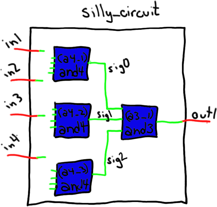
I spared you the horror of seeing all the wire criss-crossings.
The inputs are all going to each of the and4 units.
Here’s the module:
1
2
3
4
5
6
7
8
9
10
11
12
13
14
15
16
17
18
19
20
21
22
23
24
25
26
27
28
29
30
31
32
33
34
35
36
37
38
39
40
41
42
43
ENTITY silly_circuit IS
    PORT ( in1, in2, in3, in4 : IN BIT;
           out1 : OUT BIT);
END silly_circuit;

ARCHITECTURE struct OF something_else IS
    SIGNAL s0, s1, s2 : BIT;

    COMPONENT and4_gate IS
        PORT ( in1, in2, in3, in4 : IN BIT;
               out1 : OUT BIT);
    END COMPONENT;

    COMPONENT and3_gate IS
        PORT ( in1, in2, in3 : IN BIT;
               out1 : OUT BIT);
    END COMPONENT;
BEGIN
    -- maps by position:
    -- maps in1 to the first port of the and4,
    --      in2 to the second port of the and4,
    --      etc, sig0 to the last port of the and4
    a4_1: and4 PORT MAP (in1, in2, in3, in4, sig0);

    -- maps by position:
    -- maps in2 to the first port of the and4,
    --      in3 to the second port of the and4,
    --      etc
    a4_2: and4 PORT MAP (in2, in3, in4, in1, sig1);

    -- maps by named value (as PORT MAP ( to port => from signal, to port => from signal, ...)
    -- maps in2 to and4::in2,
    --      in3 to and4::in3,
    --      in4 to and4::in1, etc,
    a4_3: and4 PORT MAP (in2 => in2, in3 => in3, in1 => in4, in4 => in1, out1 => sig2);

    -- maps by named value
    -- maps sig0 to and3::in1,
    --      sig2 to and3::in2,
    --      sig1 to and3::in3,
    --      out1 to and3::out1
    a3_1: and4 PORT MAP (in1 => sig0, in3 => sig1, in2 => sig2, out1 => out1);
END struct;
The last takeaways of this code is:
- We named the
and4’s and theand3in oursilly_circuit, just like we had to name the signals, because they aren’t basic gates. - The architecture is named
structfor structural style, which involves (structurally) building up logic with smaller components, as we are doing here. - A common confusion is how the names don’t clash here.
You might see all the
in1’s and such and wonder whichinNis referring to what? Well earlier I mentioned that each module exists in its own little world. The names exist in their own little world, too (called scope). When we’re in our architecture body, we’re in oursilly_circuitworld, so thein1refers only to the actual input, as expected. Remember, the only reason we have theCOMPONENTdeclaration is so that VHDL knows to go out and find that module somewhere. The names in the component declaration are only for matching against the original module. - There’s two different way to map signals to our instances.
- The first way is positional. Each signal just maps directly to the first, second, third, etc port on the component. Obviously if we had more signals listed than ports, we’d get an error.
- The second is way is by naming which port is getting mapped to. This is generally clearer, but more verbose, and it won’t matter what order you put the signals in the list.
- If we were to mismatch the direction of the port mappings, and map our input to a component’s output, VHDL would give us an error. BUT, if we mismatched ports with the same type and direction, we’d just get really wonky behavior from our circuit…or not! So double check your ports!
And that’s it! This isn’t an exhaustive explanation of building circuits in VHDL. In the coming weeks, we’ll learn how to compose simple circuits to build more complex circuits that can do math like or handle logic like checking if a thirsty soda-lover entered enough money into a soda machine.
Where is VHDL?
VHDL is the language we use to describe the circuit. We need another piece of software to actually simulate that circuit and observe its functionality. In this class, we’ll use ModelSim both for coding and simulating. If you want to use ModelSim at home, you can download a version from the ModelSim website.
-
The introductory digital design and VHDL class I’ve had to TA (ECE-200) attracts students with a wide variety of backgrounds. While some students learn just fine with the provided tutorials and labs, others can be turned off by them. Even then, students tend to miss some fundamental concepts when going through the motions of the labs. As such, I’ve decided to provide a quickstart guide with a slightly different flavor. Other primers exist, but I wanted to make something a bit friendlier. This is not meant to be a full reference. I’m very loose with my language throughout this document because of the target audience. If you need to know something specific please find a more complete reference. ↩